


A complete installation walkthrough covering disassembly, SoC ribbon cable placement, DAT0/CMD/CLK/RST wiring, 3.3V and GND points, IHS modification, testing, and troubleshooting.
Disclaimer
Modifying your Nintendo Switch Lite may permanently damage the console if performed incorrectly, and will void Nintendo’s warranty. This guide is for educational purposes only. If you’re not confident in your microsoldering ability, seek a professional technician.
Introduction
Unlike unpatched Switch consoles that use the RCM fusee-gelee exploit, modchips enable custom firmware on all Switch models — including fully patched units — by performing CPU voltage glitching to bypass bootROM firmware verification. When glitching succeeds, the chip launches a payload.bin file from your microSD card in place of Nintendo’s normal boot process.
The only community-supported RP2040 modchip is Picofly (which includes pre-made variants as well as DIY builds using an RP2040-Tiny development board). “HWFLY” and “SX Core/Lite” chips exist but are not covered here.
One important note before you begin: the Switch Lite requires a microSD card to be inserted at all times once modded. Without one, the console will be unusable unless your chip’s firmware supports bypassing sdloader (e.g., Picofly firmware does support this via holding a volume button at power-on).
Tools & Materials Required
Soldering Iron
Temperature-controlled, small tip, capable of reaching 350°C consistently.
Quality Flux
Essential for clean solder flow on fine pads. Don't skip this.
34–38 AWG Wire
Single-core Kynar wire recommended. Thinner is better for routing.
Screwdriver Bits
+00 Phillips and Y1.5 tri-point for the Switch Lite chassis.
Isopropyl Alcohol
95–99% IPA to clean thermal paste off the SoC before soldering.
Thermal Paste
Non-conductive. Reapply to the SoC die during reassembly.
Soldering Tin
Leaded solder recommended; unleaded works at higher skill levels.
Kapton Tape
Optional but recommended to protect solder joints from thermal paste.
Double-Sided Tape
For securing the modchip to the IHS after installation.
Microscope
Optional but strongly recommended for inspecting SoC ribbon joints.
Toothpicks / Q-Tips
For removing thermal paste from between the SoC capacitors.
STEP 01
Disassemble the Nintendo Switch Lite
- Remove the rear shell screws and lift off the backplate.
- Remove the metal shield/cover beneath the backplate.
- Disconnect the battery connector before touching anything else on the board.
- Remove the heatpipe and heatsink assembly.
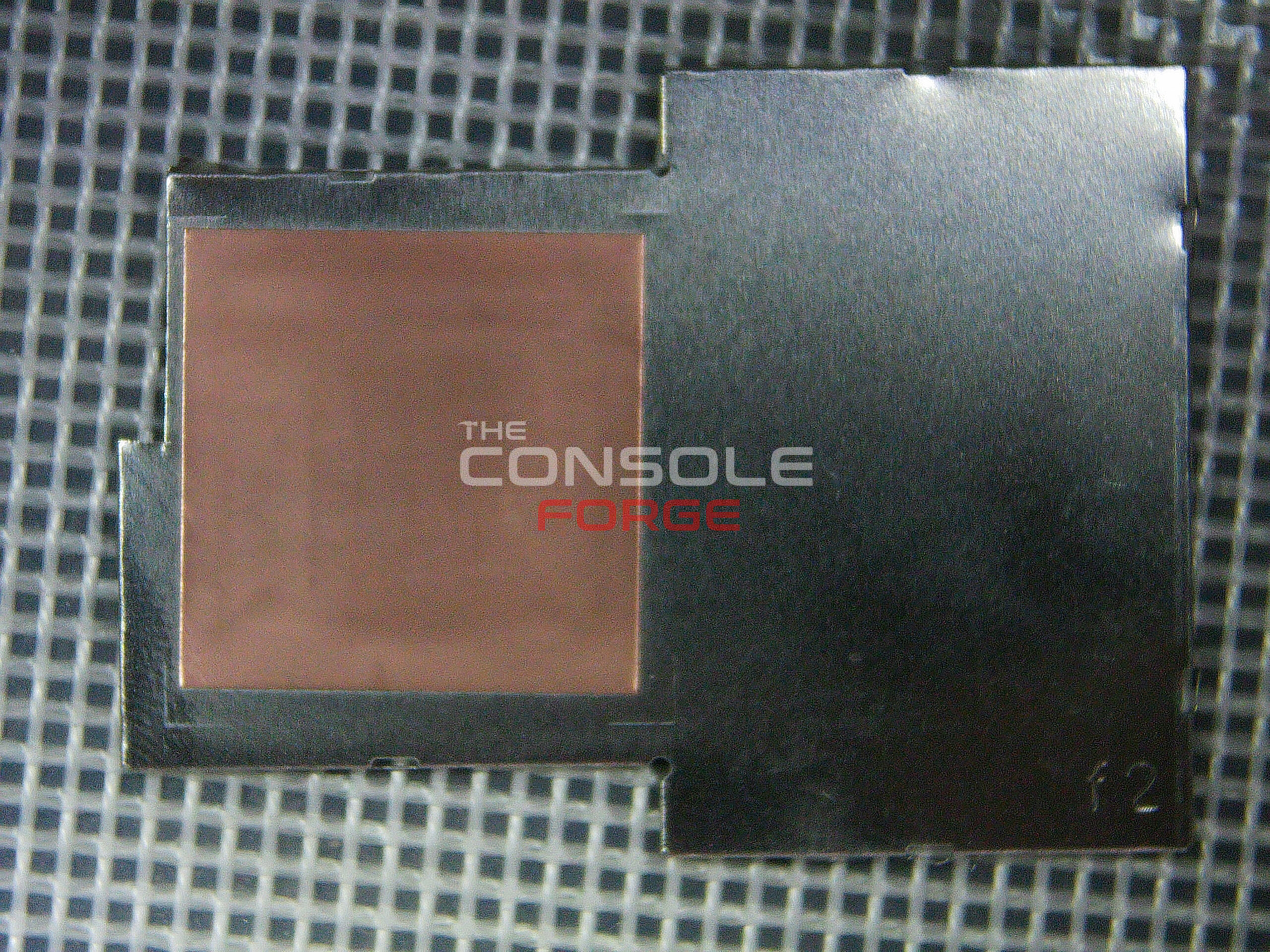
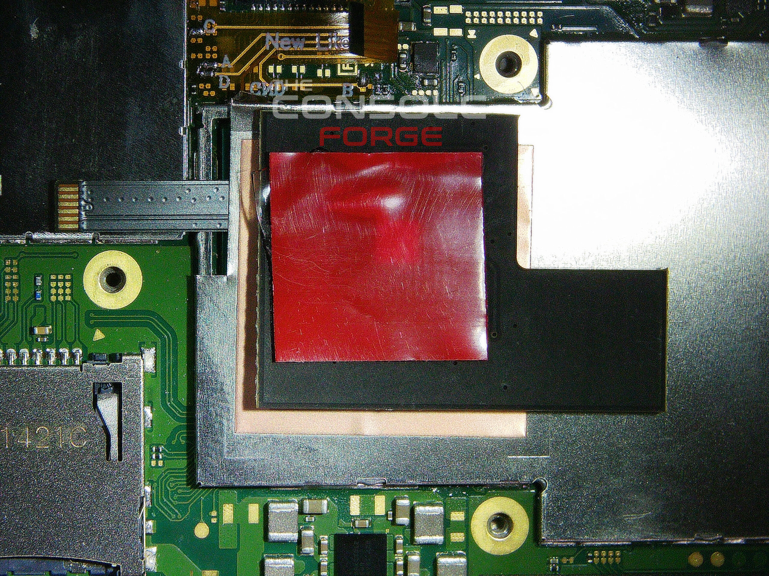
- Remove the IHS (Internal Heat Spreader) to expose the bare Tegra X1 SoC die and RAM chips underneath.
- Clean all thermal paste off the SoC die and from between the capacitors on the SoC using 95–99% IPA. The red-ish thermal goop between the heatpipe and metal shield can be left alone.
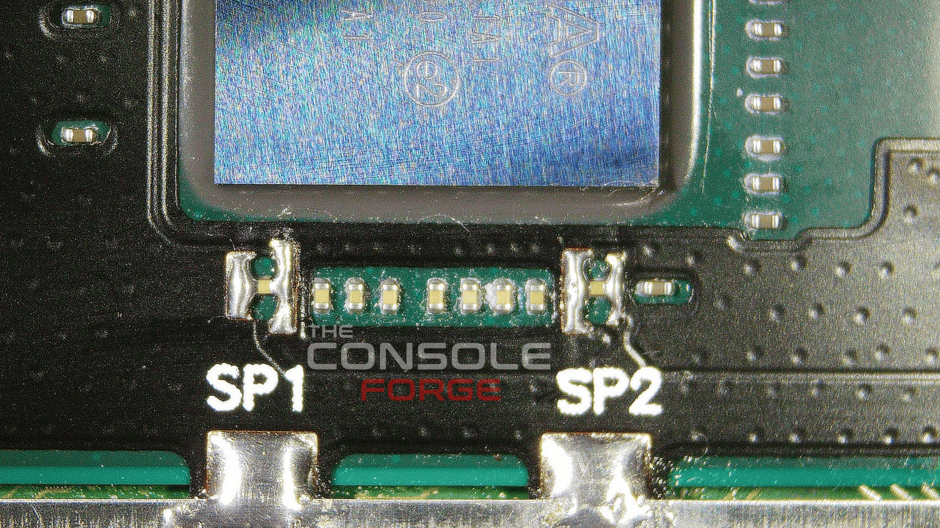
STEP 02
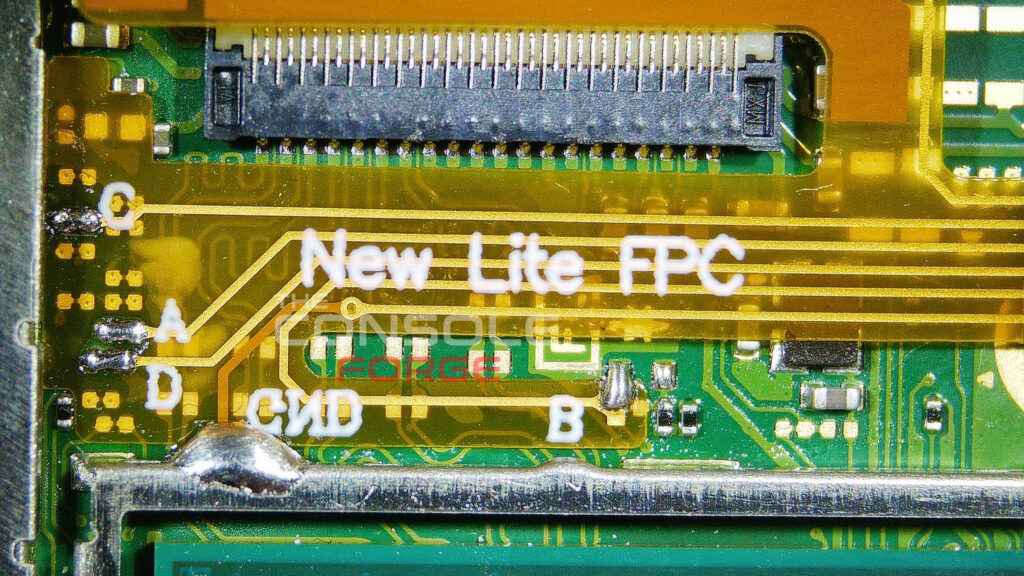
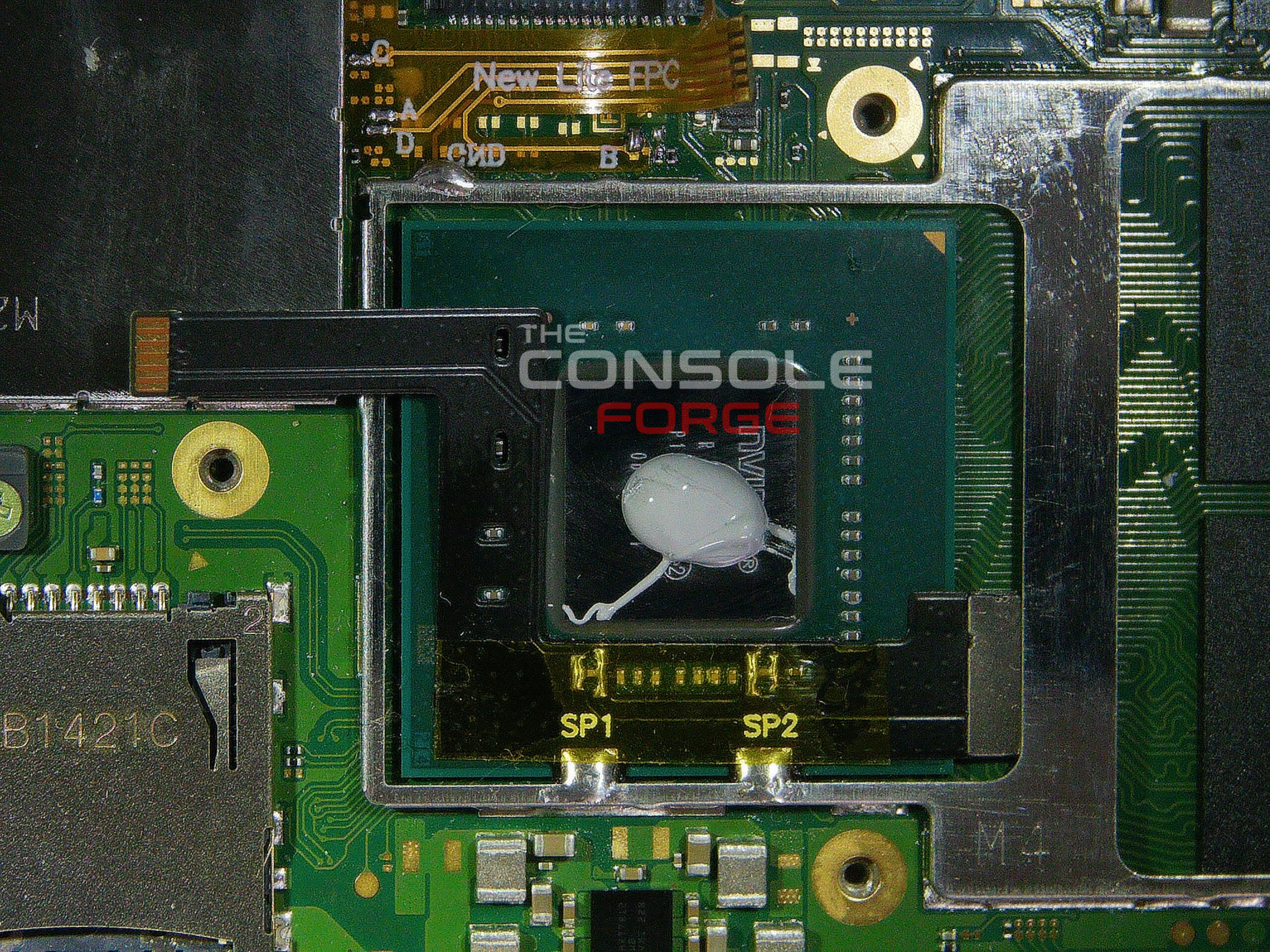
Install the SoC Ribbon Cable (CPU Flex)
SP1 and SP2. This is the mechanism that performs CPU voltage glitching. - Place the SoC ribbon cable and align it with the capacitors on the SoC die.
- Tuck the anchor points underneath the metal frame below the SoC. The MOSFET section of the ribbon cable goes underneath the frame between the SoC and RAM.
- Apply flux and use your iron to heat up each end of the capacitors at the
SP1andSP2points simultaneously with the pads on the ribbon cable. Ensure solder flows between them. - Optionally, place Kapton tape across your solder joints to prevent thermal paste from corroding them during reassembly.
STEP 03
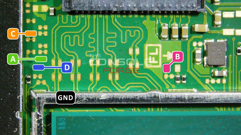
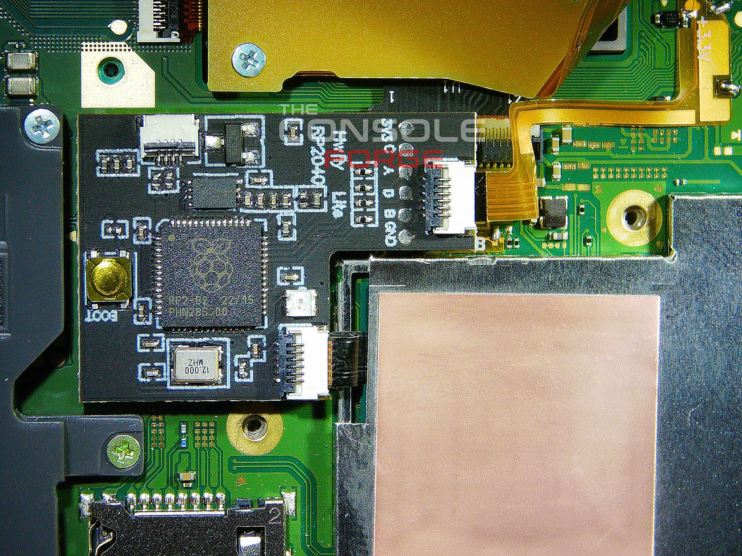
Identify & Understand the Signal Points
| Label | Signal | GPIO (RP2040-Tiny) | Notes |
|---|---|---|---|
| C | DAT0 | Pin 29 | eMMC data line — most critical point |
| A | CMD | Pin 28 | eMMC command line; solder directly to pad |
| D | CLK | Pin 27 | Clock line; solder directly to pad — no solder mask scraping needed on the Lite |
| B | RST | Pin 26 | Reset line; pad located above the SoC |
| — | 3.3V | 3.3V pin | Use exposed pads directly to the right of RAM |
| — | GND | GND pin | Any ground; recommended: "arrow" above left antenna |
| Point | +Probe to GND | −Probe to GND |
|---|---|---|
| SP1 | ~0.125 | ~0.125 |
| SP2 | ~0.12 | ~0.10 |
| A (CMD) | ~0.470 | ~0.875 |
| B (RST) | ~0.405 | OL |
| C (DAT0) | ~0.435 | ~0.450–0.850 |
| D (CLK) | ~0.440 | ~0.880 |
| 3.3V | ~0.445 | ~0.850 |
STEP 04
Solder Points C, A, D, B, and GND
- C (DAT0): Apply flux, tin the wire and pad lightly, solder. This is the most critical point — a poor joint here is the most common cause of failed boots.
- A (CMD): Apply flux, Solder directly to the A pad.
- D (CLK): Apply flux, Solder directly to the D pad. No scraping or prep needed on the Lite.
- B (RST): Apply flux, Large open gold pad above the SoC — apply flux, tin, and solder directly. No prep needed.
- GND: Any ground point on the board can be used. The recommended location is the metal shielding border surrounding the SoC, which provides a large and reliable ground connection point. Don't forget to use flux.
STEP 05
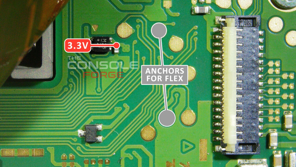
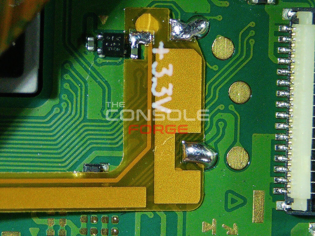
FPC Cable Anchors and 3.3V
The FPC anchor pads secure the ribbon cable to the board. The 3.3V point is soldered to the capacitor shown in the picture located to the left of the RAM chips, clearly labeled on the FPC overlay.
- Ensure the ribbon cable anchor points are properly soldered down on both sides of the SoC capacitors.
- 3.3V: Solder your wire to the large exposed 3.3V point.
STEP 06
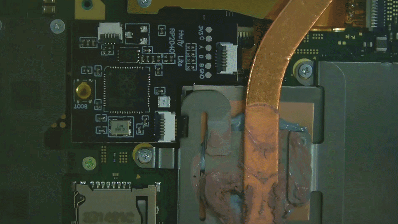
Modify the IHS and Wire Up the Modchip
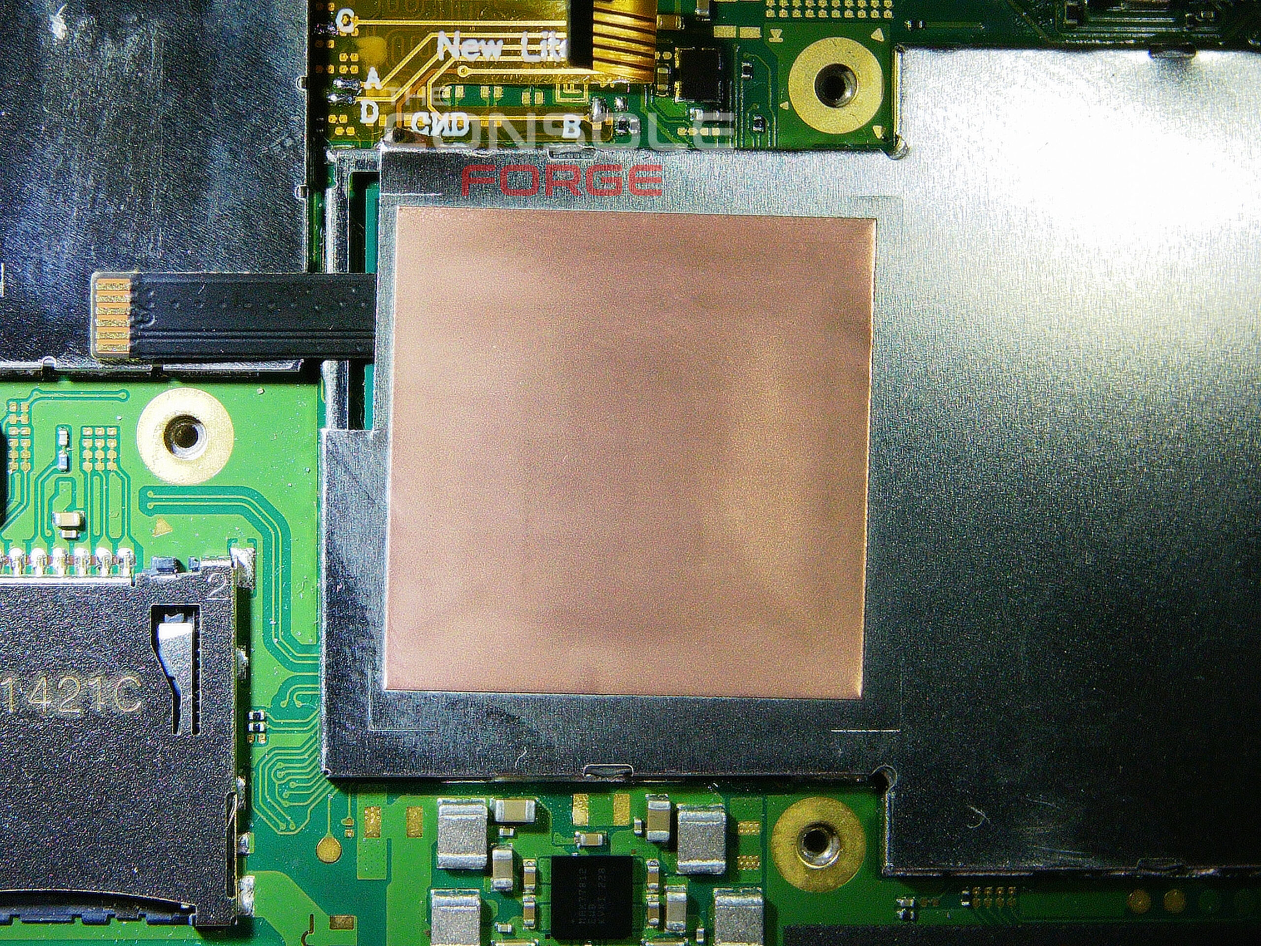
- Modify the left side of the IHS so the SoC ribbon cable can exit through the left side of the IHS housing.
- Reinstall the IHS with fresh non-conductive thermal paste on the SoC die.
- Wire up all signal lines (C, A, D, B, 3.3V, GND) to the modchip.
- Secure the modchip to the IHS using double-sided tape.
You will need to cut a strip out of the left section of the metal shield — regular scissors work fine for this.
STEP 07
Test the Installation
- Reconnect the battery connector.
- Power the console on. The modchip LED should pulse blue then solid white then, blue pulses (active glitching), then flash green once (glitch success). LED colors may vary depending on chip version,
- The console should reach a No SD Card splash screen with the Picofly logo.
- Insert a properly configured microSD card with
payload.binand verify it boots into your custom firmware. - Important: Reaching the No SD Card screen alone does not confirm full success. Test HorizonOS (stock firmware) boot too — power off, hold both volume buttons, and press power. Release volume buttons when the Nintendo logo appears. If it fails to reach the HOME Menu, check your solder joints.
Troubleshooting
Common Issues & Causes
| Symptom | Likely Cause |
|---|---|
| LED blinks red error code | Glitching/training failure — check SP1/SP2 ribbon cable joints and all signal wires |
| No SD Card screen, but fails to boot HOS | Marginal solder joints — good enough to glitch, not enough for stable eMMC communication |
| Black screen / no response | SoC ribbon cable misaligned or SP1/SP2 joints bridged to adjacent caps; check under magnification |
| Intermittent or unreliable boot | Loose wire, cold solder joint, or CMD/CLK resistor partially lifted from the board |
| CMD not connected error (short–long blink) | Bad CMD solder joint or bridge on SP1/SP2 pads; re-examine under microscope |
| Console won't power on at all | Possible accidental short to ground; check all solder points for bridges with a multimeter in diode mode |
Final Thoughts
Wrapping Up
A successful Picofly RP2040 installation on a Switch Lite requires careful preparation at every stage: thoroughly cleaning the SoC before placing the ribbon cable, scraping only what needs scraping on the CLK via, treating the CMD resistor with a light touch, and verifying diode readings before power-on. The steps are methodical, but the margin for error on some joints — especially SP1/SP2 and CMD — is small.
If something goes wrong, the troubleshooting methodology is your friend: isolate whether the issue is the ribbon cable (SP1/SP2) or the signal wiring (C/A/D/B) by removing and re-adding parts of the circuit systematically.
For detailed error code lookup and advanced troubleshooting, refer to the official NH-Switch Modchip Installation Guide troubleshooting page.